Overview
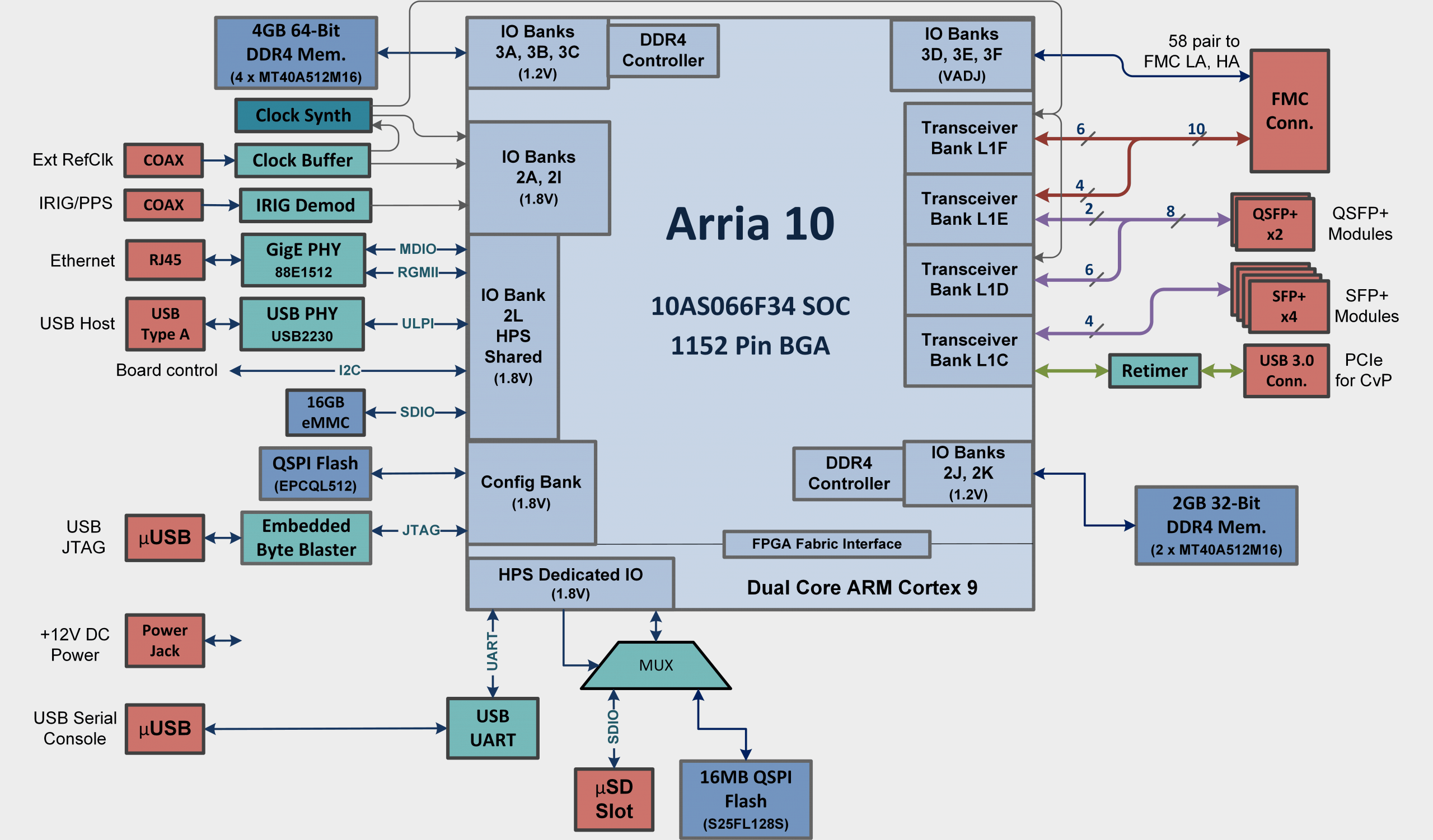
The Intel Arria 10 SoC Development Platform is designed for rapid development of high performance networking applications or process intensive applications. All networking interfaces reside on one edge of the board while the control and power interfaces reside on the opposite edge. This connector arrangement allows the COTS Altera Arria 10 SoC Development Platform to be used inside a 1U enclosure for benchtop or rackmount installations for deployment into production. The board is powered from a single 12V power supply.
Features
- Intel Arria A10 SOC (10AS066) standalone module
- Networking centric design
- FMC mezzanine slot for application flexibility
- Standalone (8.5” x 6.75”) module
- 1U enclosure available
- Complete FPGA support package available
- Full suite of Ethernet IP cores available
Interfaces and Functions
Front Panel Interfaces
-
- Dual QSPF+ ports for 40G interfaces
- Quad SFP+ ports for 10G/1G interfaces
- FMC interface with partial HPC support; All LA, HA and 10 Serdes lanes routed to FPGA
- Max VADJ of 1.8V on LA, HA signals; DIP switch selectable for 1.2V, 1.5V and 1.8V
- 5 – 200MHz external reference clock input
- 1PPS or IRIG-A/B/G input
HPS Configuration and Memory Interface
-
- HPS side 2Gbyte 32-bit DDR4 DRAM bank
- On-board 1Gbit QSPI Flash memory
- On-board socket for uSD memory card
- On-board 16Gbyte eMMC storage device
- DIP switch selectable booting from on-board QSPI, uSD card, or FPGA fabric including CvP
On-board Development and Debug Support
-
- On-board reset pushbutton and configuration DIP switches
- Multiple on-board diagnostic and status LED’s
- On-board I2C monitor access to main power regulators
- On-board I2C access to clock synthesizer and programmable oscillators
- Module and SoC on-die temperature monitoring
Rear Panel Control and Debug Intefaces
-
- GiGE interface to the Arria SoC HPS
- Type A USB 2.0 Host port to the Arria SoC HPS
- Micro-USB port for serial console access to the HPS processor
- Micro-USB port for integrated ByteBlaster II access to the FPGA / SoC JTAG port
- 1x PCIe Gen2 slave (CvP capable) interface via USB3.0 interface connector
FPGA Configuration and Memory Interface
-
- FPGA side 4Gbyte 64-bit DDR4 DRAM bank
- 512Mbit QSPI Flash device
- On-board PCIe connection to allow CvP configuration of the FPGA fabric over PCIe
Clock and Synchronization Functions
-
- Flexible clocking to allow operation of interfaces at multiple rates
- Front panel input for 5MHz-200MHz external reference clock
- Front panel IRIG A/B/G (AM and DLCS) or 1PPS interface
Power Tree
-
- Single 12V power connecter
- Adheres to Altera’s recommended Arria10 power-up and power-down sequencing
Applications and Target Markets
- Rapid Prototyping
- Low to mid volume Production
- OEM and white label
- Signal Processing / Imaging Processing
- Wireline / Wireless / RF Communications
- High Performance Computing
- 1G / 10G / 40G Wire-Speed Encryption / Decryption
- High-speed trading and Financial
Product Brief
Download to get additional info


