Agilex eSOM7 5G/Wireless Development Platform
MaxLinear
Supported MaxLinear Development Kits
- MxL1600/MxL1602 (BlackComb)
- MxL155x/Mxl165x (Matterhorn)
Overview
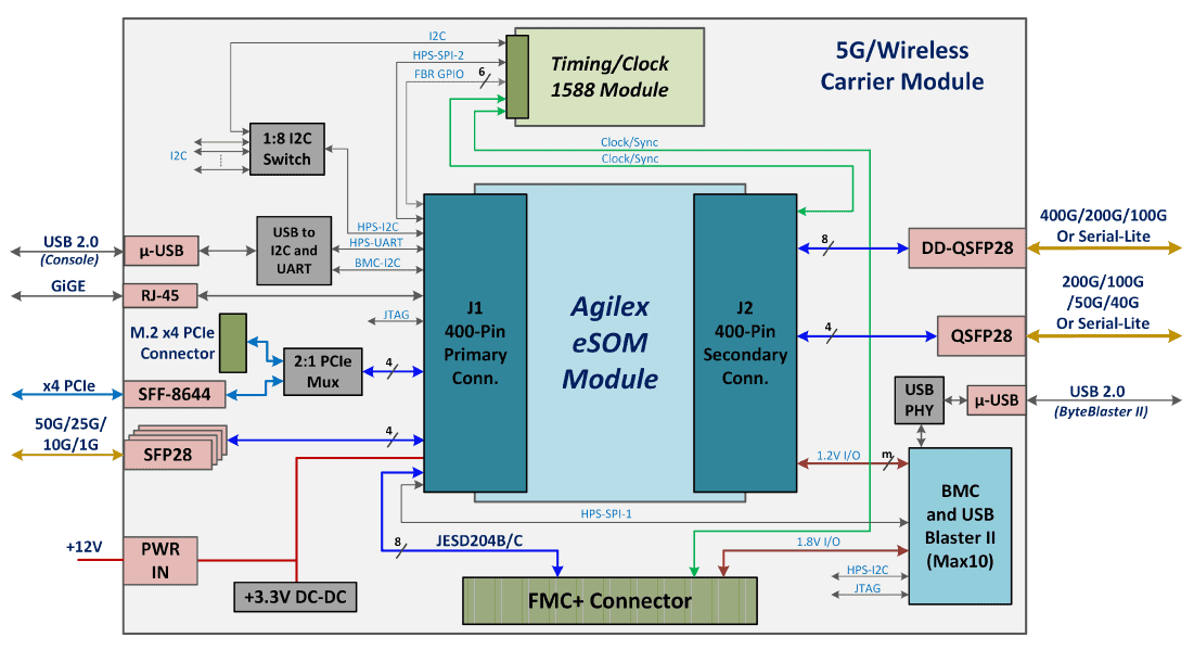
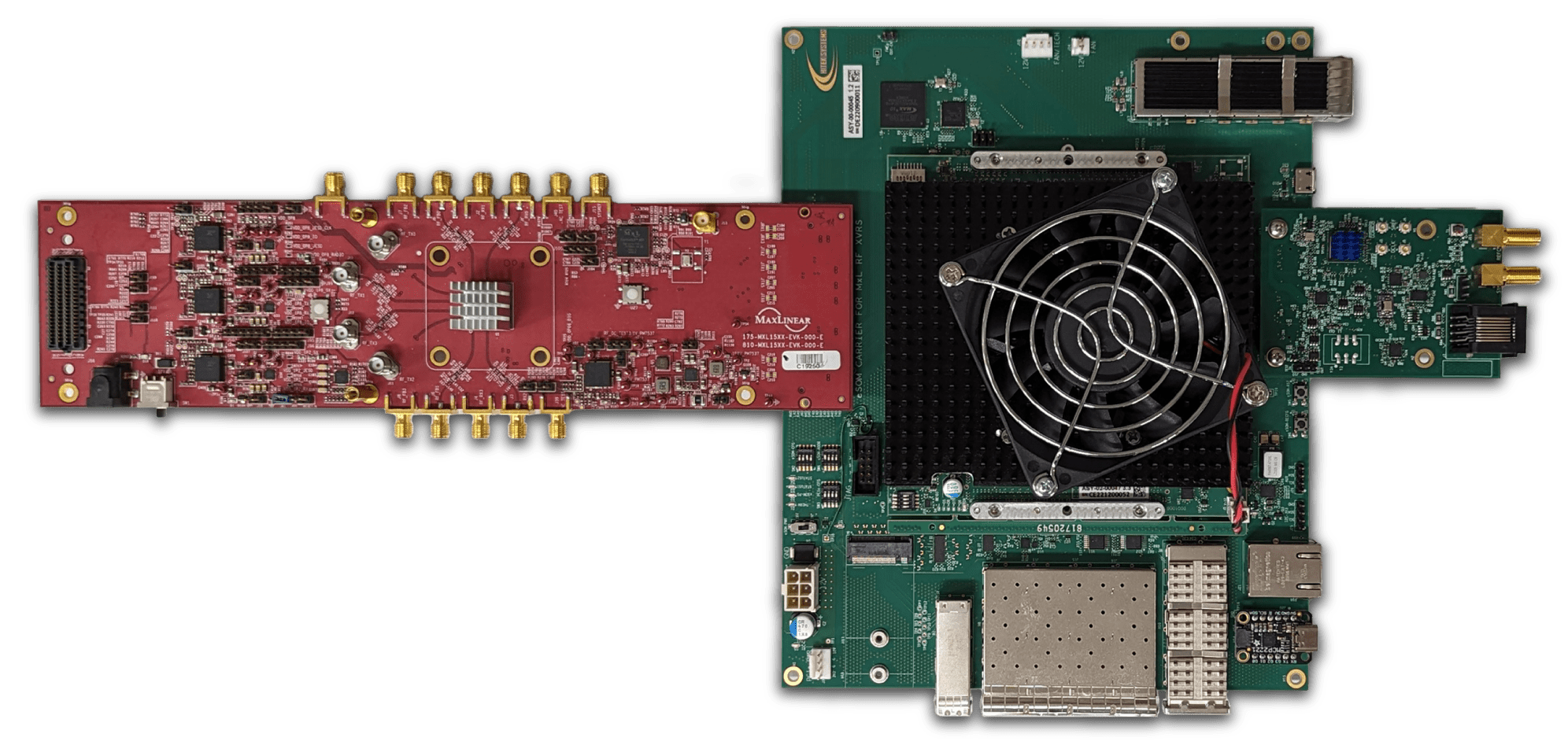
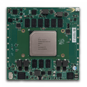
The Agilex eSOM7 5G/Wireless development platform provides a quick evaluation and prototyping platform for 5G ORAN and wireless solutions based on the Intel’s latest high performance 10nm Agilex F-Series FPGAs. The development platform consists of two modules, an Agilex 7 F-Series FPGA based eSOM7 (embedded System On Module) board with two 400-pin high speed mezzanine connectors and a carrier board which implements breakout of the FPGA serdes and I/Os. The carrier module provides a VITA57.4 FMC+ connector with level translation and control logic to interface with Maxlinear RF transceiver development kits.
Features
- Compact 8.5” x 7.0” carrier for Agilex eSOM7 FPGA module
- Supports interchangeable eSOMs with different Agilex devices; primarily designed for Agilex 7 series FPGAs with 1x and 2x F-Tiles
- Designed to provide End-to-End connectivity for 5G, Wireless and Satellite-Hub developments
- VITA57.4 FMC+ connector for RF transceiver evaluation modules
- 8 Serdes lanes up to 32 Gbps for JESD204B/C connectivity
- JESD clocks and SYSREF signals mapped to FPGA’s true LVDS IOs
- Control, configuration and I/O with level translation mapped through Max10 CPLD on carrier to support targeted evaluation modules
- Network interface connectors
- 4 x SFP28 connectors with support for 10G/25G/50G Ethernet and eCPRI interfaces
- One QSFP28 4 QSFP28 connector for networking up to 200G Ethernet
- One QSFP-DD connector for high performance networking up to 400G Ethernet
- Selectable x4 Gen4 (16Gbps) PCIe Gen4 interface
- SFF-8644 connector for x4 PCIe target to Agilex FPGA
- x4 PCIe master interface through a M.2 connector
- Resistor steering based highly configurable carrier clocking network
- Integrated USB Blaster II debug interface through micro-USB connector
- 50-pin connector for network synchronizer and interface expansion modules
- Signals mapped to eSOM HPS to support SPI, I2C and UART interfaces
- Differential clock and synchronization signals to support PTP/1588 and SYNCE based network synchronization including JESD 204B/C clock generation
- Processor and debug interfaces
- HPS Ethernet 1000Base-T via RJ45 connector
- HPS UART and BMC I2C to the USB2.0 connector via USB to UART+I2C bridge
- HPS I2C to the carrier I2C expansion switch and carrier CPLD
- HPS mater SPI to the carrier CPLD with support for FMC+ SPI expansion
- 6-pin ATX connector for +12V power input
Product Brief
Download to get additional info
Platform Boards
FPGA Board
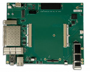
5G/Wireless Carrier
Optional Add-Ons
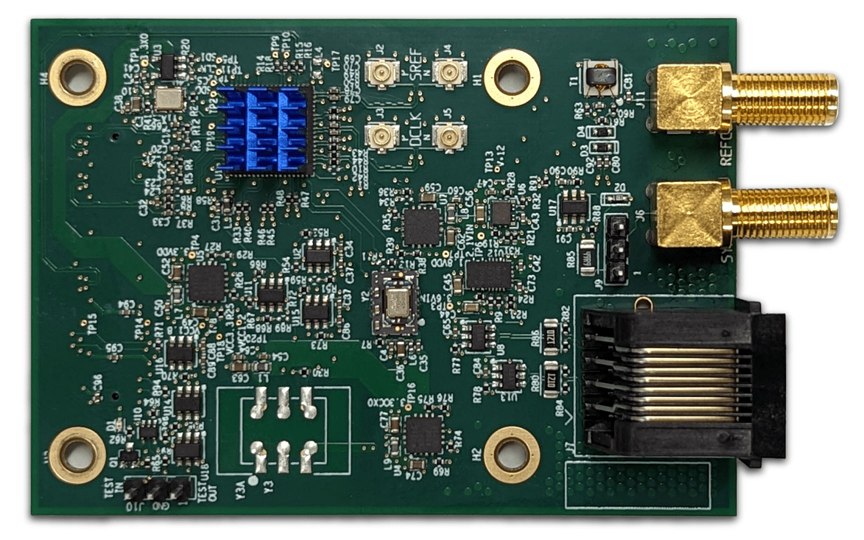
Network Synchronizer Timing Modules

eSOM Framework for ORAN Development
Features
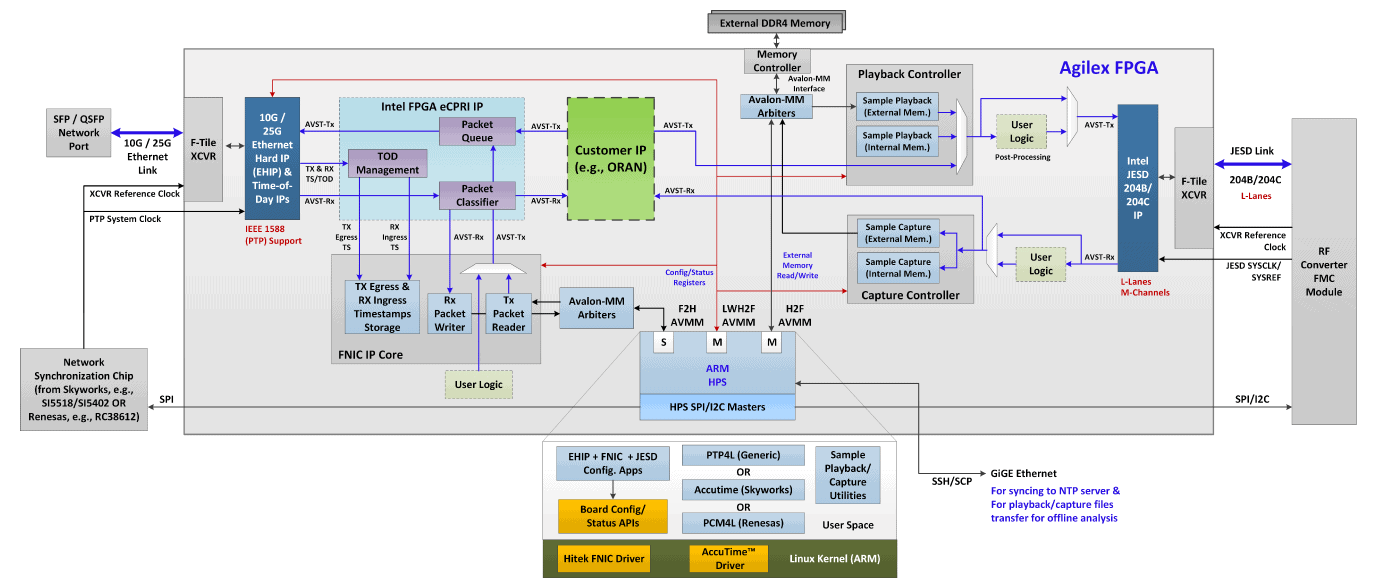
- Integrated JED204C Intel FPGA IP (with F-Tile) configured for supported RF-XVR/ADC/DAC devkits
- N-Channel (up to 8) Playback Controller with support for samples playback from FPGA internal memory or external DDR4 memory
- N-Channel (up to 8) Capture Controller with support for samples capture in FPGA internal memory or deep captures in external DDR4 memory
- Multiplexing logic for user custom pre-processing and post-processing logic at JESD Tx(DAC) path
- Multiplexing logic for sample capture at JESD Rx interface before or after user custom processing in ADC path
- External memory controller and Avalon-MM Arbitration
- Avalon-MM slave and Address decoder for configuration/status registers on HPS LWH2F interface
- Avalon-MM HPS H2F interface for burst read/write access to external memory (for sample playback/capture files)
- ARM HPS (Hard Processing Subsystem) with Linux support
- Software utilities and tools for sample playback and capture support

